Rapid Raman Quality Analysis of CVD Graphene Directly on Growth Substrates
Mathieu Monville¹*, Alexander Rzhevskii², Subarna Banerjee¹, Karlheinz Strobl¹
¹CVD Equipment Corporation, 1860 Smithtown Avenue, Ronkonkoma, NY 11779, USA
²Thermo Fisher Scientific, 800 Middlesex Turnpike, Billerica, MA 01821, USA
Abstract
Raman spectroscopy is commonly used as a standard quality analysis technique for graphene characterization since it allows unambiguous, high-throughput, nondestructive identification of the number of graphene layers. It also allows to qualify defect, doping, strain, disorder and chemical modifications levels, as well as to locate grain boundaries of graphene. Many of these quality parameters need to be monitored during process and/or scale up development of graphene material production.
Quality of graphene grown by using a Chemical Vapor Deposition (CVD) process is typically reported in the literature only after the catalyst substrate material has been removed through chemical etching followed by transfer of the resulting graphene onto another, typically Raman signal enhancing substrate. Such a transfer process usually takes many hours of time and reduces the quality of a given CVDgraphene film, making it more difficult to get reliable quality information of a given CVD graphene synthesis process run. Therefore it is desirable to find a way to analyze the type and quality of a CVDgraphene film directly on its growth substrate.
In this paper we report that Raman signals of CVD graphene can now be acquired and analyzed directly at multiple locations on the original growth substrate, thus significantly accelerating, simplifying and improving the accuracy of respective graphene quality analysis. Raman spectra were obtained from multiple substrate locations using a standard Thermo Scientific confocal Raman DXR microscope equipped with 532 nm laser to evaluate the uniformity of a given CVD graphene synthesis process. To compensate for the locally varying fluorescence background signal acquired from the metallic substrate (Fig.1) together with the CVD graphene film Raman signal, we developed a custom, self-adjusting, background subtraction routine thereby providing a background signal free Raman spectrum without human intervention. To validate our custom Raman signal processing routine, we compared the processed spectra of CVD graphene acquired directly from the growth substrate with the signal obtained after the graphene film has been transferred onto a 285nm SiO2/Sii substrate (Fig.2). Similar D/G and 2D/G intensity peak ratios were found for both the initially grown and transferred CVD graphene. To further improve the processing speed we implemented our Raman signal processing routine into the Thermo Scientific OMNIC software using Macros Basic scripting language thus allowing to spatially map the quality of graphene over large substrate area in typically less than half-an-hour time (Fig.3).
Figures
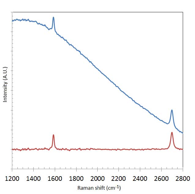
Fig 1: Example of a Raman spectrum of CVD graphene grown on Cu foil: 1) raw signal, 2) baseline corrected signal.
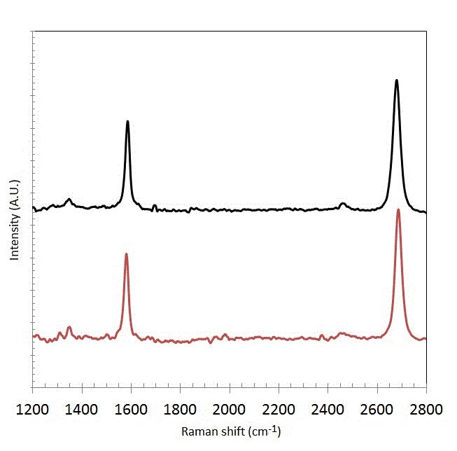
Fig 2: Comparison of Raman spectra of CVD graphene grown on Cu foil: a) baseline corrected signal obtained for as-grown graphene on Cu foil, b) raw signal obtained for graphene transferred to 285nm SiO2 / Si substrate.
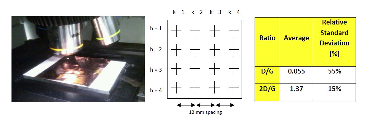
Fig 3: Spatial mapping of Raman data acquired directly on a CVD graphene film grown on a 50x50mm catalyst Cu foil : the sample is sitting on the automatic X-Y-Z stage of the Thermo Scientific DXR Microscope whose 10X objective spot light (left) can be observed at reference position (1,1) of the 4x4 data acquisition matrix (center). Raman signal acquisition, processing and translation of the stage to the various data acquisition coordinates takes less than 30 minutes in order to get standard D/G and 2D/G ratios that allow to assess the local and average CVD graphene type and quality (right) of the extended growth surface.
Presentation
 Loading...
Presented by Karlheinz Strobl at Nanotech 2012 in Santa Clara, CA
Comments are closed.