
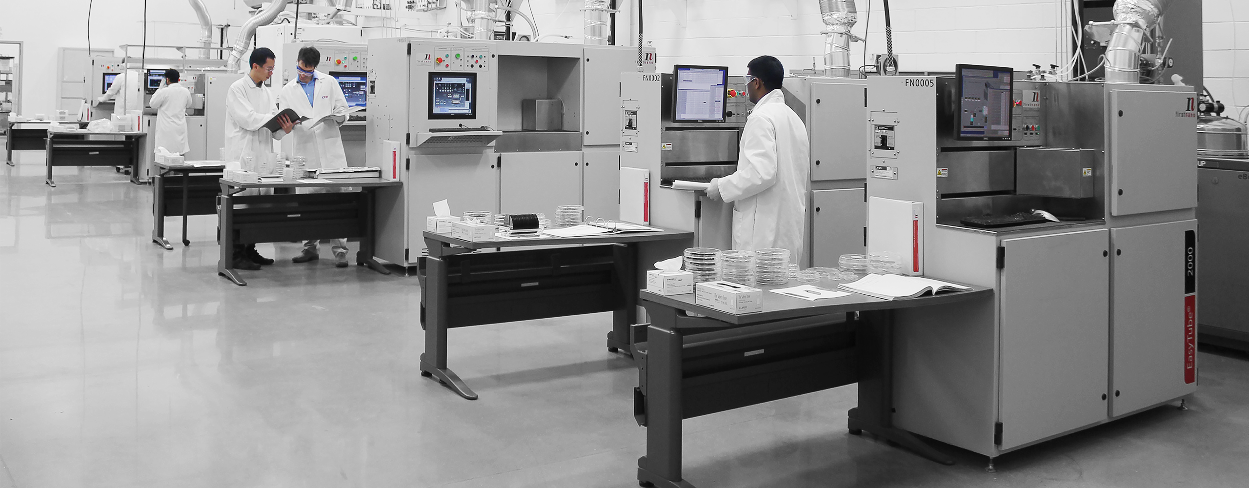
Our Electronic Materials group has developed next generation process equipment for vapor deposition and crystal growth processes for semiconductor and optoelectronic applications. As an added service to our customers we operate this equipment in our CVD Materials Corporation facility. It is here that we optimize the processes and produce advanced semiconductor materials for the electronics industry. As the equipment developer, we provide value in the quality of performance at a competitive cost.
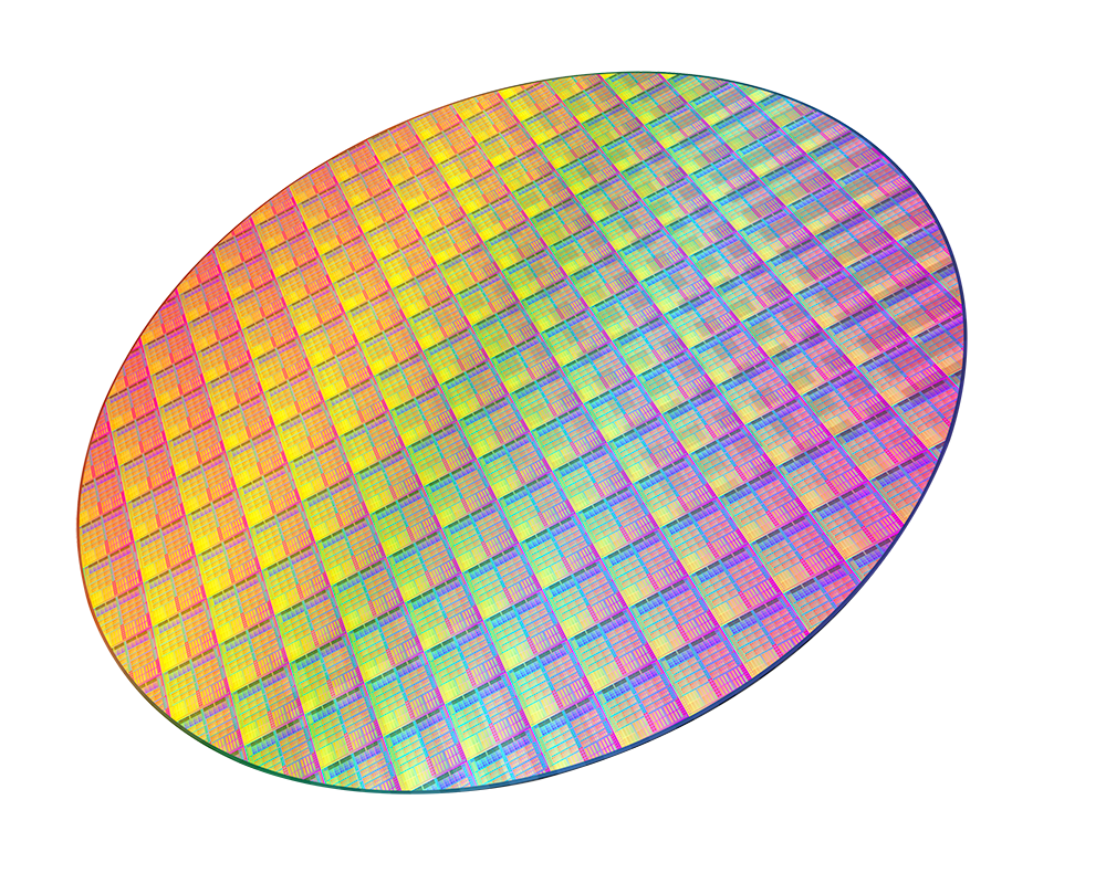
Semiconductors are crystalline compounds that form the foundation of many devices that are widely used in everyday life, including integrated circuits, optoelectronic and photonic devices, and micro-electro-mechanical (MEMS) systems.
Chemical vapor deposition (CVD) processes are used for producing semiconducting thin films and complex layered micro- and nano-structures. The CVD processes are versatile and are used to produce homoepitaxial and heteroepitaxial electronic materials as well as polycrystalline and amorphous electronic materials. A high level of compositional and dopant control can be achieved for fine tuning of the electronic properties.
Common Semiconductors
Common semiconducting materials include silicon, germanium, arsenic, antimony, etc. They can be formed in binary, ternary, and quaternary compounds with metals such as aluminum, gallium, and indium. They can also be in the form of oxides, nitrides, and carbides. Semiconducting materials are chosen for specific properties that can be exploited to realize a particular device.
Wide Bandgap Semiconductors
Wide bandgap semiconductors, such as silicon carbide (SiC), gallium nitride (GaN), and diamond, are being developed for emerging electric utility and power electronics applications. Complex semiconductor structures such as multi-layer stacks, nanowires/nanorods, and quantum dots can also be produced using CVD processes.