Novel Nanocarbon-Based, Lightweight, Flexible EMI Shield
K. Strobl* , M. Monville*, S. Banerjee*, S. Chang*, C. Jayasinghe**, J. Sprengard**
*CVD Equipment Corporation, 355 South Technology Drive, Central Islip, NY 11722, USA
**General Nano, 1776 Mentor Ave, Ste. 170, Cincinnati, OH 45212, USA
ABSTRACT
Electromagnetic interference (EMI) shielding relates to the property of a material that acts as a barrier to the penetration of electromagnetic radiations. EMI shielding plays an important role in fields of application where electromagnetic waves, especially at high frequencies, can interfere with electronics. Applications of EMI shielding span from cellular phones and computers to aerospace industry (coax cables shielding). Effective EMI shielding solutions that not only provide excellent EMI shielding but can be lightweight and mechanically reliable are sought in order to meet today's society demand for reliable electronic devices in spectral bands that spans across the MHz and GHz ranges.
In the aerospace industry, weight is a dominant factor that governs the design of most of the materials that one can find on a plane. EMI shielding materials are not an exception.
In this paper we present the first results obtained for two nanocarbon-based EMI sheets manufactured via CVD Equipment Corporation’s proprietary NanotoMarco™ manufacturing route. The two materials produced, having surface density of 20 and 40 g/m2, show high conductivity, EMI attenuations at 10 GHz similar to that of a 15μm aluminum foil (even for the case of the ½ lighter 20g/m2 sample) and good mechanical properties, demonstrating that our manufacturing platform can compete with existing, alternative technologies to provide lightweight EMI shielding solutions for the aerospace industry.
Keywords: electromagnetic interference (EMI) shielding, composite materials, nanocarbons.
1 INTRODUCTION
1.1 EMI shielding
1.1.1 Absorption and reflection of incident radiation
EMI shielding has two causes: absorption or reflection of the incident electromagnetic wave [1].
Reflection is made possible by mobile charge carriers (electrons or holes), which interact with the electromagnetic wave. Metals, with their sea of free electrons are therefore natural candidates as EMI shielding materials. Electrical conductivity is not specifically required for shielding, as non-percolated conductive networks can act as shields. Yet shielding is enhanced by connectivity. Silver, copper, gold, and aluminum are excellent for reflection, due to their high conductivity. When considering lightweight materials, metallic films, thin foils or wire braids are often used. However, they can break in height vibration environments due to metal fatiguing effects. Multiple reflections will enhance shielding effect; therefore porous metallic foams with high surface area (SA) are potentially interesting material candidates.
Electromagnetic wave absorption occurs through the action of electric and/or magnetic dipoles within the shielding material. In this case, materials with low value of dielectric constant and/or high magnetic permeability typically perform better.
In terms of materials properties, magnetic and electric field shielding relates respectively to permeability μ and permittivity ε of the shielding material.
1.1.2 Skin effect and shielding effectiveness
Adding up all losses, whether from reflection, absorption, or multiple reflections, gives an overall loss called the shielding effectiveness (SE) of a given material (expressed in dB): the greater the absolute value is, the better the shielding effect.
Electromagnetic theory of conductors shows that, at high frequencies in the GHz range, electromagnetic radiation penetrates only the outer “skin” of an electrical conductor. This is known as the “skin effect”: the electric field of a plane wave penetrating a conductor drops exponentially with increasing depth into the conductor. The depth at which the field amplitude is divided by e compared to the incident amplitude is called the “skin depth” δ, which is given by:
where
ω, angular frequency of the alternative current created by the wave of frequency f : ω = 2πf ,
μ, permeability of the material
ε, permittivity of the material
ρ, its resistivity, ρ = 1/σ,
σ, its conductivity.
The design of an effective lightweight electromagnetic interference shielding material at high frequency (making sure approximation of angular frequencies well below 1/ρε applies) is therefore governed by:
- the key parameters that take part in the skin effect: the electrical conductivity σ of the material, its magnetic permeability μ, the frequency f of the electromagnetic wave of interest and the thickness d of the material relative to the corresponding skin depth δ ,
- the total surface area of the material SA (m2/g),
- the density of the material.
In our case, we are looking for a high surface area, metallic-like, electrically and mechanically interconnected lightweight material that can be manufactured economically in the tens of microns range, is mechanically strong enough to be usable in automatic cable manufacturing equipment and has a skin depth value δ that is about 3-5 times smaller than the material thickness d at the targeted frequency f in order to obtain a sufficiently large EMI shielding value (> 65 dB) at a given low material surface density (g/m2).
1.2 Nanocarbons for EMI shieding
New forms of nanocarbon-based materials can provide novel solutions for the above framed material specifications. Even though they may not be as conductive as metals typically used for such an EMI shielding application (for example aluminum, copper or silver), carbon materials can be attractive as EMI shielding materials since carbon is chemically inert (resistance to oxidation), thermally stable, and has low density compared to metals. Nanocarbons attractiveness lies in the fact that nanocarbons can be manufactured in forms that are suffiently conductive, have high surface area and can form mechanically and electrically interconnected networks acting as a multiple reflections medium for the incident electromagnetic waves.
Flexible graphite foils in the thickness of 3mm have been shown previously to provide very high EMI attenuation capability 129 dB, for example at 2GHz [2]. The thin and flexible pyrolitic graphite material sold under the trademark PGS by Panasonic [3] manufactured with a combination of polyimide and exfoliated graphite in principle fits the above requirements, with the exception that it requires 3000K processing temperatures and high pressure [4] to achieve its 17-25 μm thick PGS sheets which makes it hard to cost-efficiently scale to larger sheet sizes. The all carbon nanotube-based EMI attenuation sheet manufactured by Nanocomp [5] also fits most of the above specified requirements, but its fully vertically manufacturing process is throughput limited, thereby making it difficult to reduce the material cost even in volume production.
1.3 NanotoMarco™ transformation process
1D, 2D or 3D nanomaterials and the transformation from their nano form to a solid macro format provide a multitude of options for designing and manufacturing novel materials for given applications. To solve the challenges of tomorrow regarding energy saving, energy storage, water purification and others, multifunctional, low-cost materials are needed that can be optimized in a multidimensional design parameter space and manufactured economically at the same time. Practically, this translates into creating effective functional materials with less matter, enhanced properties, and simpler processing.
CVD Equipment Corporation has recently prototyped in its Application Laboratory a general purpose NanotoMarco™ transformation process, which is capable of transforming a wide range on nanomaterials (carbon and non carbon-based) into macroscopic forms (for example sheet form) utilizing a combination of low temperature process steps in a volume scalable and cost efficient manner and which can be optimized to create a wide variety of multifunctional materials that can be tuned for different applications. By separating the raw nanomaterial manufacturing process from the “Nano-to-Marco” material transformation process one gains additional material design and material processing options that allow now 1) the manufacturing of a much larger type of nano-enabled macroscopic material formulations and 2) to manufacture them typically more economically than is possible with either a vertical integrated manufacturing process and/or manufacturing process requiring high temperature processes step.
We utilized this NanotoMarco™ transformation process to design and manufacture a novel nanocarbon-based EMI material suitable for the proposed application.
2 EXPERIMENTATION
2.1 Preparation of nanocarbon-based samples
Both samples where designed and manufactured by CVD Equipment Corporation utilizing their NanotoMarco™ transformation process using either nanocarbon materials manufactured within its Application Laboratory or by outside suppliers (for example General Nano) as raw materials.
2.2 EMI shielding effectiveness characterization set-up
General Nano performed all of the here shown characterization data of the respective EMI shielding material samples.
The EMI SE values versus the frequency of the incident electromagnetic wave was determined for our novel nanocarbon sheet by using a waveguide test setup and an Agilent network analyzer with a frequency test range capability ranging from 5GHz to 20 GHz. Measurements for our nanocarbon-based EMI shield materials were carried out between 8 to 15 GHz. Figure 1 shows more details of the test setup used to get the below shown EMI shielding data. All analysis were performed under identical testing environment to facilitate comparison of data. During the EMI measurement, each nanocarbon sheets was placed between two horn type waveguides that were then clamped together. The dimension of the open slit in the waveguide was 56.2mm x 9mm.
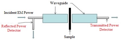
Figure 1: Schematic drawing showing waveguide measurement apparatus for our nanocarbon sheet.
2.3 Mechanical tests
Mechanical testing of samples was also performed by General Nano.
Tensile tests were performed using an Instron 3345 tensile tester with a 5 N load cell (Figure 2). Each nanocarbon sheet sample was mounted with a scotch tape (Figure 2, inset) on a perforated paper strip made with a puncher. Strain information is calculated from the actual grip displacement as tensile force is applied. The load and the displacement data are generated and automatically saved on the computer.
In our current tests, the pulling rate of the system was 1 mm/min and we used a 9.5 mm gauge length. The tensile strength of each nanocarbon sheets was calculated by dividing the load with the cross section area of each respective sample. Average width and thickness of each samples were measured before the test with a high resolution microcaliper.
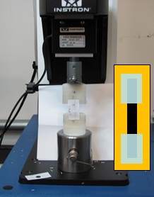
Figure 2: Nanocarbon sheet mounted on the Instron machine for tensile testing (inset sketch shows the nanocarbon-based sheet specimen taped on paper).
3 RESULTS AND DISCUSSION
3.1 EMI shielding effectiveness (SE)
EMI SE results, recorded from 8 to 15 GHz, are shown on Figure 3 (0 dB means no shield, shielding effect gets stronger as absolute values gets higher). Overall shielding effectiveness reaches -65dB over this bandwith with spikes at -90dB. As expected, the thicker material (sample A, 22μm, 36g/m2) provides more shielding (-10dB in average) compared to the thinner material (sample B, 15μm, 23 g/m2).
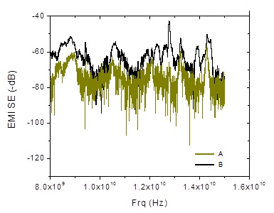
Figure 3: EMI shielding effectiveness of the two test samples A and B, from 8 to 15 GHz.
On Figure 4, one can see that EMI attenuations around 10 GHz are similar to that of a 15μm aluminum foil (even for the case of the ½ lighter 20g/m2 sample, sample B). Values at the point of interest of 10 GHz are included in Table 1.
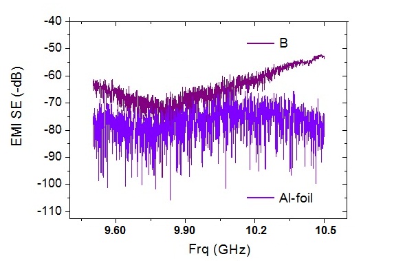
Figure 4: EMI shielding effectiveness of 15μm thick sample B (20g/m2) compared to 15 μm thick Al foil around 10 GHz. Stress vs Strain curves for samples A and B are shown in Figure 5.

Figure 5: Tensile Stress vs. Strain curve for the two test samples A (40g/m2) and B (20g/m2).
Table 1 below summarizes the types of samples that were analyzed and the results obtained for the two types of measurements that were performed. Additional basic 4-point probe characterization data reveals high conductivity for both samples.
| sample designation | [type] | A | B | Al foil |
| mass/area | [g/m2] | 36 | 23 | 41 |
| thickness | [µm] | 22 | 15 | 15 |
| density | [g/cm3] | 1.6 | 1.6 | 2.7 |
| electrical conductivity by 4 point probe method | [S/cm] | 3,800 | 5,600 | - |
| EMI attenuation @ 10 GHz | [dB] | 77 | 74 | 80 |
| tensile | [MPa] | 26 | 50 | - |
Table 1: Summary table of properties of our high and low mass/area test samples.
4 CONCLUSION
These first results demonstrate that despite choosing only low temperature processing steps and a non-vertically integrated, but therefore more scalable and flexible manufacturing route (NanotoMarco™), a novel nanocarbon-based lightweight EMI shielding material manufacturing process could be designed and manufactured that can compete in performance with the existing alternative technologies. This novel manufacturing process is projected to be more affordable and easier to volume scale-up.
REFERENCES
[1] D.D.L. Chung, "Materials for Electromagnetic Interference Shielding", J. Mater. Eng. Perf. 9(3), 350-354, 2000.[2] X. Luo and D.D.L. Chung, "Electromagnetic Interference Shielding Reaching 130 dB Using Flexible Graphite", Carbon, 34(10), 1293-1294, 1996.
[3] PGS Panasonic Product Data Sheet, 2012.
[4] US Patent US20110045300A1, 2011.
[5] Miltary & Aerospace Electronics, February 2010, 12-23, 2010.
Poster
 Loading...
Presented at NanoTech 2013 in Washington, D.C.
Comments are closed.