Nanocarbon-based Material Platform for the Manufacturing of Multifunctional Materials
Mathieu R. Monville1, Kongara M. Reddy1, Riju Singhal1, Karlheinz Strobl1
1CVD Equipment Corporation, 355 South Technology Drive, Central Islip, NY 11722, USA
Introduction
The field of nanocarbon-based composite materials is naturally driving and stimulating applied research today because of the high potentialities offered by both nanotechnology and carbon: each nanocarbon species (nanotubes, nanocones, nanowalls, graphene and graphite nanoplatelets, fullerenes and carbon nanodots, etc.) presents its own specific physico-chemical properties and reacts and performs differently under the same conditions, thereby enabling the optimization of material properties for specific applications (energy storage, water desalination, lightweight conductive materials, etc.).
Using a proprietary transformation process, we were able to transform different nanocarbon species into macroscopic paper-like sheets without adding any polymeric binder
material or applying high temperature treatment. Examples are provided, representing our initial findings.
NanotoMacro™ transformation process 0D, 1D, 2D or 3D nanomaterials and the transformation from their nano form to a solid macro format provide a multitude of options for designing and manufacturing novel materials for given applications. To solve the challenges of tomorrow regarding energy saving, energy storage, water purification and other applications, multifunctional, low-cost materials are needed that can be optimized in a multidimensional design parameter space and manufactured economically at the same time. Practically, this translates into a goal of creating effective functional materials with less matter used, enhanced properties, and/or simpler processing.
CVD Equipment Corporation has recently prototyped in its Application Laboratory a general purpose NanotoMacro™ transformation process, which is capable of transforming a wide range on nanomaterials (carbon and non-carbon-based) into macroscopic forms (for example sheet form, see Figure 1.) utilizing a combination of low temperature process steps in a volume scalable and cost efficient manner and which can be optimized to create a wide variety of multifunctional materials that can be tuned for different applications. By separating the raw nanomaterial manufacturing process from the “Nano-to-Macro” material transformation process one gains additional material design and material processing options that allows now 1) the manufacturing of a much larger range of nanoenabled macroscopic material formulations and 2) to manufacture them typically more economically than is possible with either a vertical integrated manufacturing process and/or manufacturing process requiring at least one high temperature processes step.
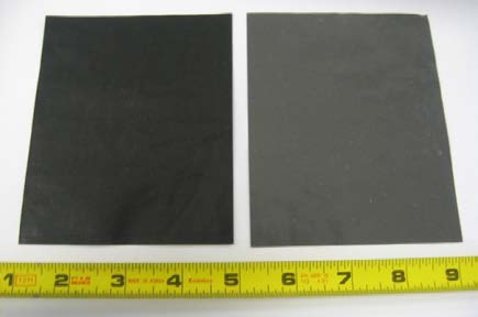
Figure 1. Two 4”x5” samples of paper-like nanocarbon sheet (left: 2-FC-50, right: 2-MD-53) created through our NanotoMacro™ manufacturing process.
We utilized this NanotoMacro™ transformation process to design and manufacture novel nanocarbon-based materials for different applications.
Nano-enabled carbon-based composite materials tuned for specific applications
Principle
We investigated the transformation of different sources of nanocarbons to make large nanocarbon-based sheets (Figure 2.), performed comparative studies focused on thermal and electrical properties (with specific attention on EMI shielding for one material) and looked at the potential for manufacturing novel electrode materials for energy storage applications. We also began to experiment with using this process for non-carbon nanomaterials.
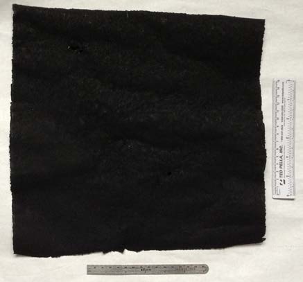
Figure 2. 12”x12” square wide sample of nanocarbon sheet type 2-FC-50.
Conductivity studies
Setups were designed for in-plane and through-plane electrical and thermal conductivity measurements per ASTM [1] and other standards (Figure 3.). Several sheets were made from different nanocarbon starting materials. Table 1 lists a few selected properties. The final sheet properties achievable depend in part on the type of nanocarbons used as raw materials and in part on the chosen manufacturing process steps.

Figure 3. Schematic front view of conductivity measurement set-ups for in-plane (left) and through-plane (right) measurements
Table 1. Example of conductive properties of different nanocarbon sheets created through our NanotoMacro™ process.
| Sheet | In-plane | Through-plane | Density | Specific capacitance (in 6M KOH) |
|---|---|---|---|---|
| Code | S/m | S/m | g/cm3 | F/g |
| 4-TG-78 | 3,511 | 126.0 | 0.49 | 42 |
| 3-TG-25 | 3,677 | 193.2 | 0.19 | N/A |
| 3-WV-40* | 3,810 | 0.2 | 1.11 | N/A |
| 4-SG-71-1 post-treated | 4,430 | 43.9 | 0.48 | 65 |
| 4-NC-02 | 14,815 | 64.7 | 0.22 | N/A |
| 2-FC-57 | 25,563 | N/A | 0.78 | N/A |
| 3-DGMD-48 | 86,580 | 27.7 | 1.18 | N/A |
| 2-MD-53-4 | 107,527 | N/A | 0.80 | N/A |
| 3-MG-27 | 179,695 | 13.9 | 0.90 | N/A |
| 2-MD-53-4 post treated | 952,381 | N/A | 0.82 | N/A |
*based on a non-carbon nanomaterial
EMI shielding composite sheet
The design of an effective lightweight electromagnetic interference shielding material at high frequency is dependent on [2]:
-the electrical conductivity σ of the material, its magnetic permeability μ, the frequency f of the electromagnetic wave of interest and the thickness d of the material relative to the corresponding “skin depth” δ ,
-the total surface area of the material SA (m2/g),
-the density of the material.
Therefore, we were looking for a high surface area, metallic-like, electrically and mechanically interconnected lightweight material that could be manufactured economically in the tens of microns thickness range, that is mechanically strong enough to be usable in automatic cable manufacturing equipment and has a skin depth value δ that is about 3-5 times smaller than the material thickness d at the targeted frequency f of 10GHz in order to obtain a sufficiently large EMI shielding value (> 65 dB) at a given low material surface density (g/m2).
Our results show that EMI attenuations around 10 GHz reach a peak value of -74dB, similar to that of a 15μm aluminum foil (in the case of a 20g/m2 sample, sample 2-B). Values around the point of interest of 10 GHz are presented below (Figure 4.)
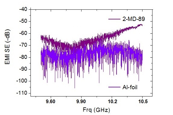
Figure 4. EMI shielding effectiveness of 15μm thick sample 2-MD-89 (20g/m2) compared to 15 μm thick Al foil around 10 GHz.
Non-carbon-based nanomaterials can outperform carbon- based materials in some applications
A change from a carbon-based nanomaterial to a non-carbon-based nanomaterial creates new varieties of nano enabled sheet materials (Figure 5.).
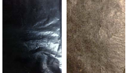
Figure 5. Two 4”x5” samples of paper-like nanocarbon-based sheet (left: 2-FC-57) and non-carbon-based nanomaterial sheet (right: 3-WV-40) created through our NanotoMacro™ manufacturing process: processing of right sample includes the usage of a non-carbon nanomaterial, resulting in a lower electrical conductivity (see Table 1.).
Conclusion
We successfully applied our NanotoMacro™ manufacturing route that we originally developed to transform a wide range of nanocarbon materials into a sheet format to also non- carbon-based nanomaterials. We demonstrated that this material transformation process has the potential to be fine-tunable for a wide range of target applications. This basic manufacturing route can be applied to a wide range of applications/markets: it is an easy-to-scale up manufacturing route, whose processing steps can be adjusted for both carbon-based and non-carbon-based nanomaterial sources and for different target applications.
Acknowledgements
We would like to thank General Nano LLC for providing us with the EMI shielding effectiveness measurements on some of our nanocarbon sheets and our several industrial partners for providing us with their carbon and non-carbon raw nanomaterials.
References
[1] ASTM C611 for in-plane sheet resistance measurements, ASTM D5470-12 for through plane thermal conductivity measurement.
[2] Chung DDL. Materials for Electromagnetic Interference Shielding, J. Mater. Eng. Perf. 2000; 9(3): 350-54.
Presentation
 Loading...
Presented by Mathieu R. Monville at the Rio Carbon 2013 Conference in Rio de Janeiro
Comments are closed.