Low-Cost, High-Volume Scale-Up of CVD graphene on Cu Foil
Karlheinz Strobl, Mathieu Monville, Riju Singhal, Samuel Wright, Leonard Rosenbaum
CVD Equipment Corporation, 355 S. Technology Drive, Central Islip, NY 11722, USA
Abstract
Our EasyGraphene™ R&D and production tools enable our patent pending solution for low-cost, high-volume, high quality CVD graphene on Cu foil. Together our EasyGraphene™ system enables:
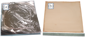
- Better thermal control over the CVD graphene process: Figure 1 (a) is a photograph of a 300 mm x 300 mm 18 µm thick electropolished Cu foil subjected to 2 hour annealing and 2 hour CVD graphene growth at 1020 °C and 15 Torr using a conventional CVD graphene system and process. Note the Cu foil is wrinkled. Its warped surface affects the quality of any post-processing (transfer, etc.). Figure 1 (b) is a photograph of a 300 mm x 300 mm Cu foil processed in an EasyGraphene™ tool incorporating our patent pending technology. Note, the Cu foil is wrinkle-free even after > 5 hours of processing time.
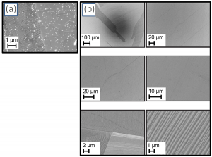
- Less contamination and less maintenance: Traditional CVD tube furnace systems used for graphene growth on Cu require frequent maintenance in order to remove Cu film deposits and to avoid particulates from polluting the graphene. Figure 2 (a) is a high magnification SEM image of CVD graphene grown in a traditional tube furnace. The ‘white dots’ are SiO2 , CuOx and other nano to micro scale particulates. Figure 2 (b) contains SEM images at low and high magnification of CVD graphene grown in an EasyGraphene TM system. We observe > 1000 X less ‘white dots’ and our maintenance cycle is prolonged by 10-100 X.
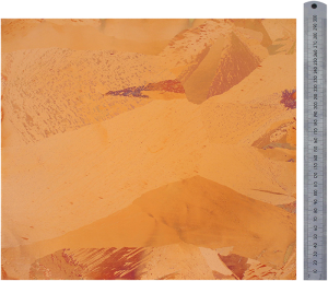
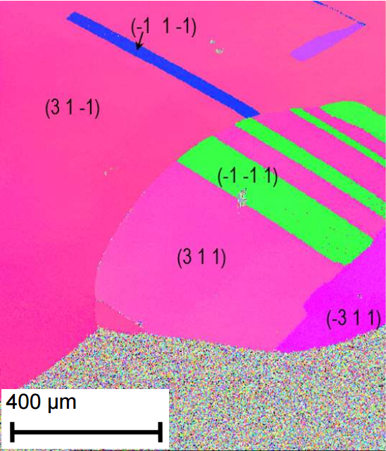
- High quality graphene over large areas, with improved uniformity: After a 1 hour thermal annealing of Cu foils using an EasyGrapheneTM system, the Cu grain size can be enlarged up to 300 mm (the full size of the foil), as can be seen in the photograph in Figure 3 below. Larger Cu grains enable the growth of high quality CVD graphene due to fewer grain boundaries and large uniform crystallographic regions of the Cu foil. Electron backscatter diffraction (EBSD) confirms the single-crystal nature of the large Cu grains (see Figure 4 below).
Our EasyGraphene™ tools enable large-area uniform graphene growth. Figure 5 below is a photograph of a 300 mm x 300 mm Cu foil with a prematurely terminated monolayer graphene growth (to obtain partial monolayer coverage). It was unloaded from the EasyGraphene™ reactor at 200 °C to rapidly oxidize the regions of Cu that are not covered by graphene. The inset is an enlarged area showing a few-mm sized hexagonal graphene islands. The graphene island size is well known to be related to local processing conditions (pressure, temperature, gas concentration): here we see the graphene island size is uniform across the whole 300 mm x 300 mm growth area.
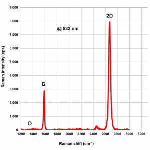
Figure 6 below is a Raman spectrum of a CVD graphene film made with an EasyGraphene™ system and transferred onto a glass substrate. The spectrum is characteristic of a monolayer graphene film with little-to-no appreciable defects.
Figures
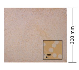
Figure 5: Photograph of 300 mm x 300 mm graphene on Cu foil sample produced using an EasyGraphene™ system. Interrupted growth with oxidation of exposed Cu foil makes the graphene grains clearly visible by eye. Inset: enlarged area showing mm-sized hexagonal graphene islands -> uniform large-area graphene growth.
Submitted to the Graphene 2014 Conference in Toulouse, France

Comments are closed.